Integrated photonics is a promising solution for addressing the rapidly growing energy demand of data traffic worldwide. By fabricating photonic integrated circuits (PICs) on traditional silicon wafers, entire photonic systems can be integrated into chips, resulting in higher speed, low thermal effects, and optimal integration capability. Silicon photonics is expected to be a key technology for data centers, with global sales projected to increase to USD 972 billion by 2027. Furthermore, integrated photonics has various applications, such as miniaturized LIDAR sensors for autonomous vehicles and micrometer-fine needles with integrated photonic circuits for targeted stimulation of fluorescence effects in living tissue. The LASER World of PHOTONICS and World of QUANTUM events will showcase the latest innovations in integrated photonics, quantum technology, automation, and robotics, making it a must-attend event for professionals in these industries.
Integrated photonics is a rapidly advancing technology that is promising for addressing the global energy demand of data traffic. The technology is finding applications in a range of fields, including data communication, aerospace sensors, autonomous vehicles, biophotonics, and medicine. Laser World of Photonics, a leading international trade fair for photonics components, systems, and applications, will bring together key players in this field in Munich from June 27, 2023.
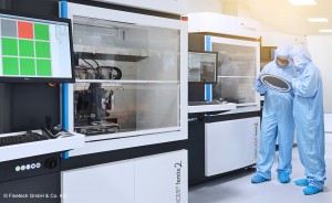
At the heart of integrated photonics is precision optics and laser technology, which is advancing chip technology beyond imagination. The EUV exposure process, developed by a team from LASER exhibitors, has already won the German Future Prize 2020. The process involves using a high-performance CO2 laser to bombard 50,000 tin drops per second with two pulses each, generating tin plasma that emits extremely short-wave EUV radiation (13.5 nm). The precision optics can direct the laser beam with such accuracy that it would be able to hit a golf ball on the moon.
The result is state-of-the-art semiconductor chips with structures in the single-digit nanometer range. While a few years ago, it was only possible to fit 10 billion transistors on a fingernail, this number is now approaching the trillion mark. This exponential growth is in line with Moore’s law, which predicts that the number of transistors in integrated circuits doubles every 18 months. However, nano-scale production is reaching its limits, and “More than Moore” concepts are required.
Integrated photonics is at the forefront of advancing chip technology into the third dimension via the 2.5-D intermediate step. However, even 3D chips will not be enough to cope with the ever-increasing data volume worldwide. Nevertheless, integrated photonics is pushing the boundaries of what is technically possible and offers promising applications in addressing the energy demand of data traffic and beyond.
Integrating photonics directly into chips, sensors, and other technical components through photonic integrated circuits (PICs) is a promising and cost-effective solution. These optical circuits can be fabricated on traditional silicon wafers, leveraging the existing infrastructure of the semiconductor industry. This approach involves using established pulse etching processes to introduce the light-based circuits into the optically “difficult” silicon, enabling entire photonic systems with laser beam sources, light guides, couplers, filters, signal modulators, ring resonators, and photodetectors to be integrated into the chips.
Achieving this level of precision on a nano scale requires hundreds of process steps and interlocking design, validation, and manufacturing processes. To make this possible, the LASER community has developed enablers such as nano-positioning technology, ultra-precise testing and measurement methods, and III-V semiconductors that selectively compensate for the photonic deficit of silicon.
Leading providers of simulation and design tools, manufacturing solutions, testing and measurement solutions, positioning technology, and semiconductors will showcase their innovations at LASER World of PHOTONICS in Munich from June 27, 2023. The event will feature a focus area for Integrated Photonics in Hall A2, as well as application-oriented presentations. The World of Photonics Congress, which will also be held in Munich, will bring together international experts to explore the potential of integrated (silicon) photonics. This technology has enormous potential, and its integration into chips and other technical components is a promising solution to address the ever-increasing energy demand of data traffic.
Replacing electricity with light in photonic integrated circuits (PICs) offers numerous advantages, including low thermal effects, optimal integration capability, and higher speed. Moreover, the spatial requirements of electronic-optical assemblies, strong heat generation, and the conversion of optically transmitted data into electrical signals are eliminated. Data transmission and processing on multiple wavelengths in multiple modes in miniaturized PICs make it a promising solution to handle the growing global data volumes more efficiently. As a result, integrated photonics has matured into a key technology for data centers, with global sales of silicon photonics expected to increase to USD 972 billion by 2027.
In addition to data centers, integrated photonics has applications in various fields, such as autonomous vehicles, healthcare, aerospace, and agriculture. For instance, miniaturized LIDAR sensors are being developed to enhance the safety of autonomous vehicles, and research laboratories are using micrometer-fine needles with integrated photonic circuits to stimulate fluorescence effects in living tissue in a targeted manner. There are also projects worldwide to develop smart implants, miniaturized diagnostic and analysis devices, and miniature sensors for different fields of application. Integrated photonics has the potential to usher in a new era of technology.
The LASER World of PHOTONICS and World of QUANTUM events will be held from June 27 to 30, 2023, at the Munich exhibition grounds, alongside automatica, the leading exhibition for automation and robotics. With just one ticket, attendees can visit all three events and explore the latest innovations in integrated photonics, quantum technology, automation, and robotics.
Don’t miss interesting posts on Famousbio


